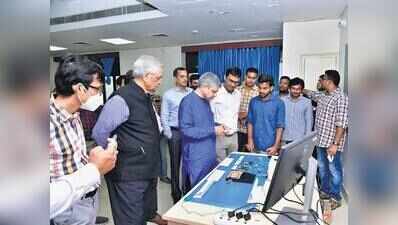
Bhubaneswar: The state govt plans to help out engineering students aspiring to design minuscule chips that power everything from smartphones and cars to medical devices. For them, access to specialised software used by semiconductor companies is often a major hurdle, which the govt seeks to remove.The electronics and information technology (E&IT) department has recently enabled 13 institutions to access advanced electronic design automation (EDA) tools free of cost under the chips to startup (C2S) programme, giving students and faculty an opportunity to learn chip design using tools closer to those used in the industry.According to the department, EDA tools are essentially digital workbenches on which chips are designed. Engineers use them to develop circuits, test whether a design works as intended, identify errors and prepare the design for the next stages of production.While students at many technical colleges receive theoretical knowledge of chip design in classrooms, access to such specialised tools can provide them with hands-on experience.“By making advanced EDA tools available free of cost to institutions, the state is seeking to lower one of the major barriers to semiconductor education which is the high cost and specialised nature of industry-grade design software. This move will give engineering students a chance to move from learning about chips in classrooms to actually designing them,” said educationist Prahallad Tripathy.He added that as semiconductor companies increasingly seek engineers trained in specialised design and verification skills, early exposure to industry-oriented tools could give the state’s engineering graduates a stronger foundation to compete for jobs in chip design and related electronics sectors.The 13 institutions include IIT Bhubaneswar, NIT Rourkela, IIIT Bhubaneswar, BPUT Rourkela, VSSUT Sambalpur, KIIT, SOA, C V Raman Global University, Silicon University, Trident Academy of Technology, Centurion University of Technology and Management, Parala Maharaja Engineering College, Berhampur, and GIET University, Gunupur.The department said the industry-standard tools would enable students and aspiring chip designers to gain practical experience in semiconductor design. The move builds on the state’s earlier implementation of the C2S programme. Last year, electronics and IT minister Ashwini Vaishnaw had announced the implementation of the programme in four institutions – IIT Bhubaneswar, NIT Rourkela, IIIT Bhubaneswar and Parala Maharaja Engineering College.The C2S programme focuses on training engineering students in semiconductor-related technologies, including embedded system design, with the broader objective of creating a skilled talent pool for India’s growing semiconductor industry.